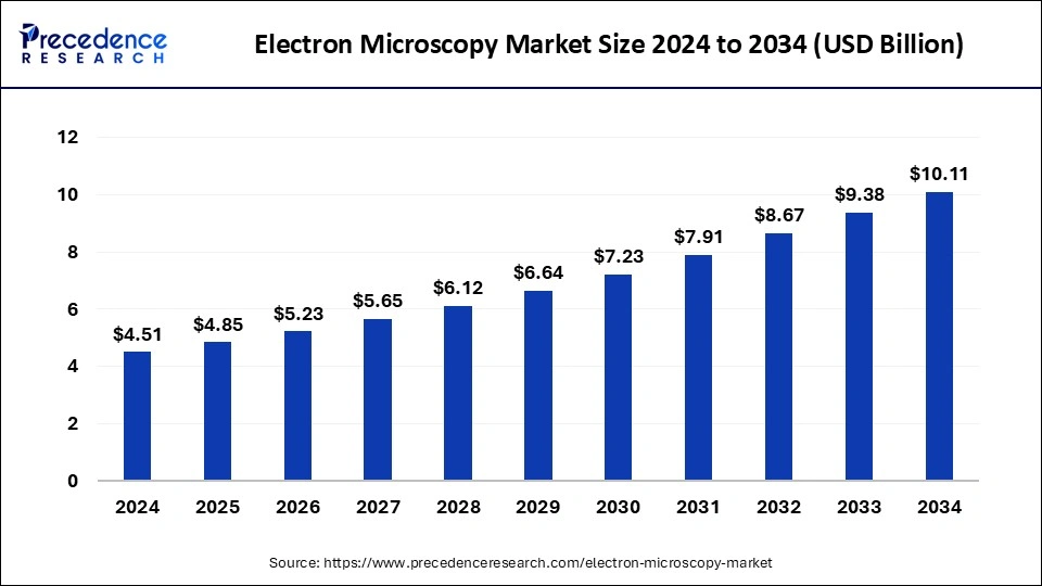
Electron Microscopy Market Size Worth USD 10.11 Billion by 2034
The global electron microscopy market size is valued at USD 4.85 billion in 2025 and is expected to be worth over USD 10.11 billion by 2034, growing at a notable CAGR of 8.50% from 2025 to 2034. North America accounted for the largest market share of 35.70% in 2024, while Asia-Pacific is expanding at a notable CAGR during the forecast period.
Ottawa, Oct. 09, 2025 (GLOBE NEWSWIRE) -- According to Precedence Research, the global electron microscopy market size is calculated at USD 4.85 billion in 2025, and it will grow from USD 5.23 billion in 2026 to nearly USD 10.11 billion by 2034.
In terms of CAGR, the market is expected to expand at a strong compound annual growth rate of 8.50% from 2025 to 2034. The electron microscopy market is driven by the increasing need for high-resolution, nanoscale imaging to develop research and development in fields such as nanotechnology, biotechnology, materials science, and semiconductor manufacturing.
The Complete Study is Now Available for Immediate Access | Download the Sample Pages of this Report@ https://www.precedenceresearch.com/sample/2959
Electron Microscopy Market Key Takeaways:
- The global electron microscopy market was valued at approximately USD 4.51 billion in 2024 and is projected to reach USD 10.11 billion by 2034.
- The market is expected to grow at a CAGR of 8.50% from 2025 to 2034.
- North America held the largest share of over 35.70% in 2024, driven by strong R&D investments and a robust base of research institutions.
- Scanning Electron Microscopy (SEM) dominated the market with a 78.70% share in 2024, due to its versatility in surface imaging and analysis.
- The Life Sciences segment led by application, accounting for 24.89% of the total market share in 2024.
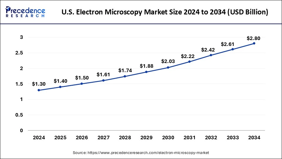
- The U.S. market was valued at around USD 1.30 billion in 2024 and is expected to reach USD 2.80 billion by 2034.
- Major growth drivers include increasing demand for nanotechnology research, pharmaceutical R&D, and advanced semiconductor manufacturing.
- Advancements in resolution, imaging speed, and detector technology are expanding microscopy capabilities into new scientific and industrial applications.
- Integration of AI, automation, and analytical tools such as energy-dispersive X-ray spectroscopy (EDS) is enhancing data accuracy and throughput.
- Asia-Pacific is the fastest-growing region due to expanding semiconductor and life science industries, supported by significant government initiatives and research funding.
-
Europe shows steady growth with increasing adoption of cryo-electron microscopy and strong government support for life science and nanotechnology research.
What is Electron Microscopy?
Electron microscopy (EM) is a scientific technique and instrument that utilizes a beam of accelerated electrons instead of light to make high-resolution images of samples, permitting the visualization of structures at a much smaller scale than light microscopy. Industries use them to analyze crystals, metals, and ceramic materials, identify faults, and ensure quality. They are utilized in the development and manufacturing of semiconductors, electronics, and other advanced materials.
Major Applications of Electron Microscopy:
- Materials Science and Nanotechnology: Electron microscopy is essential for analyzing the structure, morphology, and composition of materials at the nanoscale, aiding in the development of advanced alloys, composites, and nanomaterials.
- Semiconductor and Electronics Industry: Used for failure analysis, defect detection, and structural inspection of integrated circuits and microchips, especially as components shrink to the nanoscale.
- Life Sciences and Structural Biology: Techniques like cryo-electron microscopy (cryo-EM) allow scientists to visualize viruses, proteins, and macromolecular complexes at near-atomic resolution in their native states.
- Pharmaceutical Research and Drug Development: Electron microscopy helps visualize drug–target interactions, analyze pharmaceutical formulations, and study cellular responses to treatment at the ultrastructural level.
- Forensic Science: Scanning electron microscopy (SEM) is widely used in forensic investigations to examine gunshot residues, fibers, paint chips, and tool marks with high precision.
- Geology and Earth Sciences: Electron microscopy allows geologists to study the microstructure, mineral composition, and surface textures of rocks, minerals, and fossils for resource exploration and environmental analysis.
- Environmental Science: Electron microscopy is used to analyze airborne particles, pollutants, and bioaerosols, providing detailed morphological and elemental data important for environmental monitoring and research.
- Industrial Quality Control and Manufacturing: Manufacturers use EM to inspect surface defects, coatings, welds, and failures in high-precision components across aerospace, automotive, and metallurgy sectors.
What are the Major Trends of the Electron Microscopy Market?
- Growth of Cryo-Electron Microscopy and Structural Biology: The cryo-EM segment is expanding rapidly, especially in life sciences, as researchers demand near-native, high-resolution imaging of proteins, viruses, and cellular complexes.
- Integration of Artificial Intelligence / Automation: Electron microscopes are increasingly being paired with artificial intelligence (AI) and machine learning tools for tasks like automated image processing, particle recognition, aberration correction, and real-time data analysis to reduce human effort and accelerate throughput.
- Advancements in Detectors, Resolution & 3D / Ultrafast Imaging: Innovations such as direct electron detectors, aberration correction, high-speed cameras, and electron tomography are pushing both resolution and imaging speed, enabling 3D reconstructions and observation of dynamic processes.
- Miniaturization & More Accessible / Portable Systems: There is a rising demand for benchtop, compact, or field-deployable electron microscopes, making the technology more accessible to smaller labs, educational institutions, and industrial users.
-
Key Driving Applications: Semiconductors, Materials Science, and Pharmaceuticals: Increased needs in semiconductor R&D, advanced materials analysis, and pharmaceutical research are driving the adoption of electron microscopy across multiple high-impact sectors.
✚ Access the Exclusive Research Report ➡️ https://www.precedenceresearch.com/electron-microscopy-market
Electron Microscopy Market Opportunity
Growing Demand for High-Resolution Imaging in the Electronics and Pharmaceutical Industries
High-resolution electron microscopy is in high demand in electronics and pharmaceuticals due to the rising complexity of semiconductor components, the demand for nanoscale defect analysis, and even the pharmaceutical industry's focus on drug discovery, disease mechanism understanding, and quality control via molecular-level analysis of biological structures.
Electron microscopy is important for ensuring product quality by precisely imaging microelectronic components and even supporting the development of next-generation semiconductor technologies. By offering high-resolution imaging of cellular and even molecular structures, electron microscopy assists in understanding disease mechanisms, contributing to more effective therapies.
Electron Microscopy Market Key Challenge
Lack of Skilled Operators
The lack of skilled operators is a key challenge for the market because these developed instruments are complex, need specialized training, and generate vast amounts of data that demand expert interpretation. There is a global lack of graduate programs and dedicated training pathways that offer the necessary specialized skills for electron microscopy, creating a bottleneck in workforce development. The skill gap slows the pace of research along with innovation in fields reliant on high-resolution imaging, as institutions struggle to fully use their equipment.
Electron Microscopy Market Report Coverage
| Report Attributes | Key Statistics | |
| Market Size in 2025 | USD 4.85 Billion | |
| Market Size in 2026 | USD 5.23 Billion | |
| Market Size by 2034 | USD 10.11 Billion | |
| CAGR 2025 to 2034 | 8.50% | |
| Largest Market | North America | |
| Base Year | 2024 | |
| Forecast Period | 2025 to 2034 | |
| Segments Covered | Type, End User, Application and Regions | |
| Dominant Type Segment, 2024 | Scanning Electron Microscopy (SEM): ~78.70% Share | |
| Leading Application Segment, 2024 | Life Sciences: ~24.89% Share | |
| Regions Covered | North America, Europe, Asia-Pacific, Latin America, and Middle East & Africa | |
| Leading Region In 2024 | North America: ~35.70% of Market Share | |
| U.S. Market Size (2024) | USD 1.30 Billion | |
| Projected U.S. Market (2034) | USD 2.80 Billion | |
| Primary Growth Drivers | Rise in nanotechnology R&D; expanded uses in electronics & pharma; advancements in imaging resolution and integration with analytical modules | |
| Major Challenges / Restraints | High capital & maintenance costs; requirement for skilled operators; complex sample prep and data interpretation | |
| Technology & Capability Trends | Enhanced detectors, aberration correction, 3D/ultrafast imaging, AI/automation for image analysis, modular/compact instruments | |
| Regional Growth Trends |
|
|
➡️ Become a valued research partner with us ☎ https://www.precedenceresearch.com/schedule-meeting
Case Study: Accelerating Nanoscale Quality Control in a U.S. Semiconductor Fab
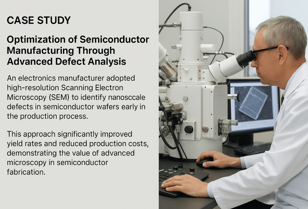
Tier-1 5-nm/3-nm fab facing yield loss from stochastic defects and line-edge roughness. Baseline inline metrology missed sub-10 nm anomalies that escaped to final test. Electron microscopy adoption aligned with market realities: SEM as dominant type, North America as the largest regional base, life-science-grade detectors crossing into semiconductor workflows, and AI/automation embedded in analysis.
Business Problem
- First-pass yield: 88.2% on leading node; target ≥92.5%.
- Root-cause cycle time for killer defects: 5–7 days; target ≤48 hours.
- Sample throughput bottleneck in FA lab: 35 samples/day; target ≥60.
Objectives
- Cut failure-analysis turnaround by ≥40%.
- Lift die yield by ≥3 percentage points within two quarters.
- Standardize nanoscale inspection for new materials stack without increasing headcount.
Solution Overview
Stack:
- High-throughput field-emission SEM with direct electron detector and automated tilt/rotate stage for 3D surface reconstructions.
- FIB-SEM for site-specific cross-sectioning of interconnects and vias.
- TEM/STEM for atomic-scale verification of barrier/liner integrity and dopant distribution.
- AI pipeline: CNN-based particle/defect classifier, unsupervised clustering for anomaly discovery, automated report generation; API bridge to MES for lot hold/release rules.
Why SEM-first: SEM delivered fastest cycle on patterned wafers, handled 80%+ of actionable flags; TEM reserved for deep-dive confirmation.
Implementation Timeline
- Week 0–2: VOC, KPI baselining, sample taxonomy, golden-defect library definition.
- Week 3–6: Tool installation, vibration/isolation commissioning, EDS integration, stage calibration.
- Week 7–10: AI model training on 120k labeled images; MLOps pipeline with continuous learning from operator feedback.
- Week 11–14: MES integration; SPC rules for auto-hold when defect clusters exceed control limits.
-
Week 15–16: Full production ramp; parallel run with legacy workflow; then cutover.
Process Changes
- Inline SEM sampling increased from 3 to 7 sites per wafer with adaptive sampling driven by AI risk scores.
- Standardized cross-section playbooks: via chain → dielectric stack → contact resistance outliers.
- Automated EDS recipes for fast elemental confirmation on suspected contamination events.
- Operator augmentation: decision assist panels showing defect probability, likely root causes, and recommended next best action.
Quantified Outcomes (6-month post-cutover)
- Failure-analysis TAT: 5.3 days → 1.9 days (−64%).
- Throughput: 35 → 72 samples/day (+106%).
- First-pass yield: 88.2% → 92.9% (+4.7 pp).
- Scrap reduction: −22% wafer scrap on affected nodes.
- Unplanned tool downtime: −18% via earlier contamination detection.
- Cost impact: ~US$14.6M annualized savings from recovered yield and reduced rework on two EUV lines.
- Time-to-root-cause for stochastic bridge defects: −58% through FIB-SEM cross-section automation.
- Operator efficiency: 1 analyst now validates 3× more cases/day via AI triage.
Technical Highlights
- Direct electron detectors increased SNR at low dose, preserving resist features.
- Aberration-corrected TEM confirmed sub-nanometer liner continuity; prevented false positives from SEM surface contrast.
- 3D SEM tomography exposed void morphology in copper fill without full TEM prep in 67% of cases.
- AI drift compensation and autofocus agents reduced unusable frames by 31%.
Governance and Quality
- GAMP-style validation for AI models; shadow mode until AUC ≥ 0.95 on hold-out lots.
- Periodic bias checks across pattern densities and illumination conditions.
- Versioned recipes and full audit trail synchronized to MES for compliance.
Lessons Learned
- SEM handles the majority of high-value decisions; reserve TEM for confirmation and materials questions.
- Label quality outranks model complexity; expert-curated defect ontologies halved false alarms.
- Adaptive sampling beats fixed recipes under process drift and new design introductions.
- Embedding EM events into SPC/MES is where savings materialize; isolated labs don’t move yield.
Transferability
- Pharma/biotech can lift cryo-EM throughput by the same AI triage and auto-reporting stack for particle picking and 2D class averaging.
- Materials labs can replicate FIB-SEM playbooks for welds, coatings, and battery interfaces to cut characterization cycles.
KPI Snapshot (Before → After)
- Root-cause cycle time: 5–7 d → ≤48 h
- Yield loss from via voids: 1.6% → 0.4%
- Confirmatory TEM per event: 3.1 → 1.2
- Analyst hours per case: 6.4 h → 2.1 h
For inquiries regarding discounts, bulk purchases, or customization requests, please contact us at sales@precedenceresearch.com
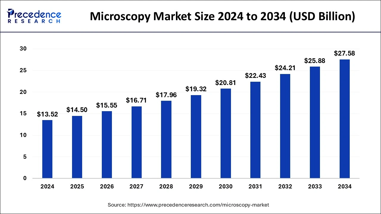
Microscopy Market – The Broader Ecosystem Powering Electron Microscopy Growth
According to Precedence Research, the global microscopy market size was valued at USD 14.50 billion in 2025 and is projected to reach USD 27.58 billion by 2034, expanding at a steady CAGR of 7.39% during the forecast period. The microscopy industry—encompassing optical, digital, and electron microscopy—forms the foundation for modern scientific imaging and research. As technological frontiers move deeper into the nanoscale, the electron microscopy (EM) segment is emerging as the most advanced extension of this broader ecosystem.
The Full Study is Readily Available | Download the Sample Pages of this Report@ https://www.precedenceresearch.com/sample/1734
How the Microscopy Market Strengthens Electron Microscopy Adoption
- Correlative Imaging (CLEM) Integration: Modern laboratories are combining optical and electron microscopy in single workflows. Optical microscopes enable quick sample screening, while EM provides nanometer-level verification—reducing analysis time and boosting research precision.
- Shared Technological Innovation: Developments in AI-based image analysis, automation, and digital detectors across the microscopy sector are now being applied to EM systems, driving higher throughput and reproducibility.
- Training and Skill Development: The global microscopy market builds the operator base that transitions into EM specialization. As universities and research centers invest in advanced imaging facilities, they create a skilled pipeline for electron microscopy.
- Cross-Industry Demand: Growth in semiconductors, life sciences, nanotechnology, and materials research fuels both optical and electron microscopy markets. The demand for high-resolution imaging naturally pushes laboratories to adopt advanced EM technologies.
- Asia-Pacific as a Shared Growth Engine: With microscopy spending exceeding USD 5 billion in 2024, Asia-Pacific is witnessing the fastest growth. Government funding in nanotechnology, semiconductor R&D, and biotechnology is simultaneously accelerating EM installations across China, Japan, and India.
- From Microscopy to Nanometrology: Traditional microscopy applications are evolving toward nanoscale analysis—bridging the gap between visualization and precision metrology. This transition directly benefits the electron microscopy market, enhancing its relevance across industries.
Market Synergy at a Glance
| Metric (2025–2034) | Microscopy Market | Electron Microscopy Market | ||
| Market Size in 2025 | USD 14.50 Billion | USD 4.85 Billion | ||
| Market Size by 2034 | USD 27.58 Billion | USD 10.11 Billion | ||
| CAGR (2025–2034) | 7.39% | 8.50% | ||
| Fastest-Growing Region | Asia-Pacific | Asia-Pacific | ||
| Key Demand Sectors | Life Sciences, Semiconductors, Nanotechnology | Semiconductors, Materials Science, Pharmaceuticals | ||
| Shared Technology Trends | AI & Automation, 3D Imaging, Portable Systems | High-Resolution Detectors, Cryo-EM, AI-Driven Analysis | ||
Immediate Delivery Available | Buy This Premium Research Report@ https://www.precedenceresearch.com/checkout/1734
How did North America Dominate the Electron Microscopy Market?
North America dominates the market with a share of 35.70% in 2024, because of significant R&D investments, a strong base of academic and research institutions, the existence of leading industry players, and even favorable government policies funding innovation in life sciences, nanotechnology, and the semiconductor industries. Rising applications in life sciences (especially cancer research, neuroscience, and drug discovery), nanotechnology, and even semiconductor manufacturing require high-resolution imaging, driving the adoption of electron microscopes.
The U.S. dominates the regional market, primarily due to its strong presence of leading microscopy manufacturers, such as Thermo Fisher Scientific, along with a robust ecosystem of research institutions, universities, and high-tech industries. The country invests heavily in R&D across sectors like life sciences, nanotechnology, semiconductor fabrication, and materials science, all of which are major drivers for electron microscopy adoption. Additionally, government funding through agencies like the NIH, NSF, and DOE supports advanced microscopy research and infrastructure. The U.S. also benefits from a well-established network of skilled professionals and advanced laboratories, making it the regional hub for innovation and commercialization in the field.
What is the U.S. Electron Microscopy Market Size?
The U.S. electron microscopy market size accounted for USD 1.40 billion in 2025 and is anticipated to reach nearly USD 2.80 billion by 2034, expanding at a healthy CAGR of 8.05% from 2025 to 2034.
Note: This report is readily available for immediate delivery. We can review it with you in a meeting to ensure data reliability and quality for decision-making.
Try Before You Buy – Get the Sample Report@ https://www.precedenceresearch.com/sample/2959
Why is Asia-Pacific the fastest-growing Electron Microscopy Market?
The Asia-Pacific is the fastest-growing electron microscopy market, driven by growing R&D investment, mainly in China, Japan, and India, which is funded by government initiatives in healthcare and technology. The region's expanding high-tech industries, such as nanotechnology, semiconductors, and even life sciences, need advanced, high-resolution imaging tools. With rising investments in healthcare, mainly after COVID-19, there is an increased demand for advanced microscopes for diagnostic purposes and even research in the life sciences and regenerative medicine.
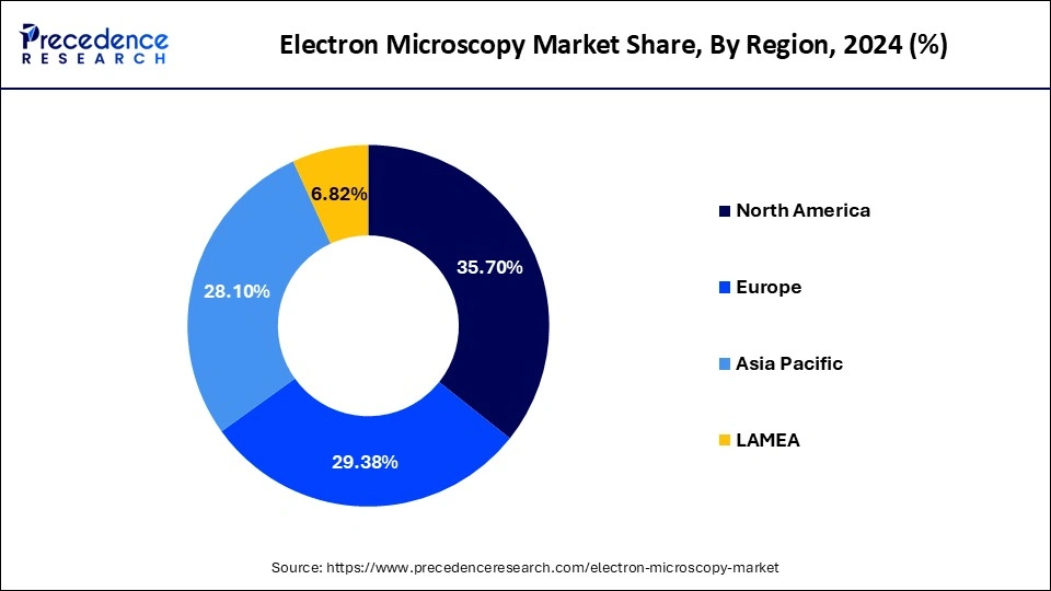
Why is Europe Showing Significant Growth in the Electron Microscopy Market?
Europe's market is rising due to robust government support for R&D, increased need for high-resolution imaging in life sciences and even nanotechnology, and the incorporation of AI and automation into microscope workflows.
High-resolution imaging is vital for precision medicine, drug discovery, and understanding complex biological structures, pushing the use of techniques such as cryo-EM. Central and Eastern European regions are showing high potential because of their expanding research capabilities and even more cost-effective environments, leading to overall market expansion.
Country-level Investments and Funding for the Electron Microscopy Industry:
- Finland - Finland’s national bioimaging research infrastructure, Euro-BioImaging Finland, received €28 million from the Research Council of Finland to upgrade imaging technologies (including electron microscopy cores) and expand services such as rapid 3D imaging of biological samples.
- European Union (multiple member states via Horizon Europe / EU research projects) - The IMPRESS project, funded by the European Commission (~€9.6 million), is developing an interoperable TEM platform with new electron sources, adaptive optics, event-driven detectors, etc., across multiple European countries.
- Spain / Catalonia (Barcelona Science Park) - The Institute for Bioengineering of Catalonia (IBEC) co-funded a new state-of-the-art (S)TEM microscope, contributing €1 million as part of a total investment of around €3.3 million.
- United States - North Dakota State University (NDSU) secured US$595,000 from the NIH Shared Instrumentation Grant Program to acquire a cryo-capable transmission electron microscope (TEM).
- Japan - The Next Generation Electron Microscopy Social Cooperation Program at the University of Tokyo (in partnership with JEOL Ltd.) is an ongoing investment initiative to develop next-generation EM methods. These include atomic resolution imaging without magnetic fields, novel detectors, high-speed EM, and 3D electron microscopy.
Electron Microscopy Market Segmentation Outlook
Type Outlook
Why did the Scanning Electron Microscopy (SEM) Segment Dominate the Electron Microscopy Market?
The scanning electron microscopy (SEM) segment dominates the market with a share of 78.70% in 2024, due to its versatility, providing high-resolution, 3D imaging of surface morphology and even composition across various fields such as life sciences, materials science, and nanotechnology. Their reliability in failure analysis, quality control, and research makes them a preferred tool for scientists and engineers. Ongoing innovation improves scanning electron microscopy functionality and even user-friendliness, supporting its widespread acceptance in both research and industrial settings.
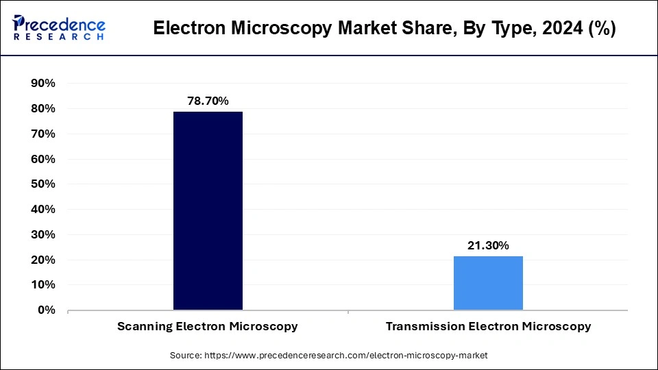
The transmission electron microscopy (TEM) segment is the second-largest segment, leading the market. The transmission electron microscopy provides superior image quality compared to the scanning electron microscope, providing atomic-scale resolution that is important for understanding materials aligning with biological structures at their most basic level. Increased investment in scientific research and development, mainly in emerging economies such as the Asia-Pacific region, fuels the need for sophisticated imaging tools such as transmission electron microscopy.
End User Outlook
Why did the Industries Segment Dominate the Electron Microscopy Market?
The industries segment dominates the market because electron microscopes are important for high-resolution imaging and even analysis in key industries such as pharmaceuticals, semiconductors, biotechnology, materials science, electronics, and mining. Electron microscopes are crucial tools for studying the structure, properties, and composition of numerous materials, including ceramics, metals, and polymers, driving the need in materials research and manufacturing.
The academic and research institutes segment is expected to grow fastest in the market during the forecast period. Due to increased investments and even funding for R&D, developments in nanotechnology and materials science demanding high-resolution imaging, the rising need in structural biology together with pathology, and expanding infrastructure in universities globally, there is a need for high-resolution imaging. Universities and even scientific organizations are expanding their infrastructure to conduct advanced microscopy work, which increases the need for electron microscopes.
Application Outlook
Why did the Lifesciences Segment Dominate the Electron Microscopy Market?
The life sciences segment dominated the market in 2024, with a share of 24.89%. The rising prevalence of chronic diseases fuels research into their molecular basis, propelling the need for electron microscopy to check disease mechanisms, tumor biology, and the effectiveness of treatments. Partnerships between microscope producers, academic institutions, and even healthcare organizations foster the advancement of specialized solutions to meet the specific requirements of the life sciences sector.
The material sciences segment is expected to grow fastest in the market during the forecast period. Due to the requirement for high-resolution nanoscale analysis of new materials, with applications in aerospace, semiconductors, and energy. Advances in nanotechnology and the rising need for novel materials with specific properties are pushing the usage of electron microscopes for detailed structural and even compositional analysis. Materials science demands the understanding of materials at the nanoscale to recognize their structure, defects, and even crystal formations, a task well-suited for electron microscopy.
You can place an order or ask any questions, please feel free to contact at sales@precedenceresearch.com | +1 804 441 9344
Top Companies in the Electron Microscopy Market
- Danish Micro Engineering (DME): DME specializes in high-precision scanning probe microscopes and accessories for electron microscopy, providing advanced tools for nanoscale imaging and surface analysis.
- Thermo Fisher Scientific: Thermo Fisher Scientific offers a comprehensive range of electron microscopes, including SEM and TEM systems, designed for high-resolution imaging and elemental analysis in materials science, life sciences, and semiconductor research.
- Hitachi High Technologies Corp.: Hitachi provides a wide portfolio of electron microscopes, known for their innovation in field emission SEMs and TEMs, catering to both academic research and industrial quality control.
- JEOL Ltd.: JEOL manufactures cutting-edge transmission and scanning electron microscopes, renowned for their high-resolution imaging and analytical capabilities across diverse scientific disciplines.
- Olympus Corp.: While traditionally focused on optical microscopy, Olympus also supports electron microscopy through integrated imaging solutions and sample preparation tools that enhance EM workflows.
- Carl Zeiss: Carl Zeiss offers advanced electron and ion beam microscopes, including Crossbeam and GeminiSEM systems, which deliver precise imaging and analytics for materials characterization and nanofabrication.
- Leica Microsystems: Leica provides industry-leading sample preparation solutions for electron microscopy, including ultramicrotomes and high-pressure freezers, enabling high-quality EM imaging.
- Nanoscience Instruments, Inc.: Nanoscience Instruments supplies a range of electron microscopy tools and accessories, including desktop SEMs and cryo-preparation systems, tailored for ease of use and educational applications.
-
Nikon Corp.: Though primarily known for optical systems, Nikon contributes to the electron microscopy field through imaging software and correlative microscopy platforms that bridge light and electron microscopy techniques.
Recent Developments:
|
|
Electron Microscopy Market Segmentation
By Type
- Scanning Electron Microscopy (SEM)
- Transmission Electron Microscopy (TEM)
- Others
By End User
- Industries
- Academic and Research Institutes
- Others
By Application
- Lifesciences
- Material Sciences
- Semiconductors
- Nanotechnology
- Others
By Regions
- North America
- U.S.
- Canada
- Europe
- U.K.
- Germany
- France
- Asia-Pacific
- China
- India
- Japan
- South Korea
- Malaysia
- Philippines
- Latin America
- Brazil
- Rest of Latin America
- Middle East & Africa (MEA)
- GCC
- North Africa
- South Africa
- Rest of the Middle East & Africa
Thank you for reading. You can also get individual chapter-wise sections or region-wise report versions, such as North America, Europe, or Asia Pacific.
Immediate Delivery Available | Buy This Premium Research Report@ https://www.precedenceresearch.com/checkout/2959
Stay Ahead with Precedence Research Subscriptions
Unlock exclusive access to powerful market intelligence, real-time data, and forward-looking insights, tailored to your business. From trend tracking to competitive analysis, our subscription plans keep you informed, agile, and ahead of the curve.
Browse Our Subscription Plans@ https://www.precedenceresearch.com/get-a-subscription
About Us
Precedence Research is a worldwide market research and consulting organization. We give an unmatched nature of offering to our customers present all around the globe across industry verticals. Precedence Research has expertise in giving deep-dive market insight along with market intelligence to our customers spread crosswise over various undertakings. We are obliged to serve our different client base present over the enterprises of medicinal services, healthcare, innovation, next-gen technologies, semi-conductors, chemicals, automotive, and aerospace & defense, among different ventures present globally.
Web: https://www.precedenceresearch.com
Our Trusted Data Partners:
Towards Healthcare | Towards Packaging | Towards Automotive | Towards Chem and Materials | Towards FnB | Towards Consumer Goods | Statifacts | Towards EV Solutions | Towards Dental | Nova One Advisor | Market Stats Insight
Get Recent News:
https://www.precedenceresearch.com/news
For the Latest Update Follow Us:
LinkedIn | Medium | Facebook | Twitter
✚ Related Topics You May Find Useful:
➡️ Automated Microscopy Market: Explore how automation and AI-driven imaging are transforming high-throughput biological and materials research.
➡️ Microscope Market: Examine how innovation in digital, optical, and electron microscopes is advancing global research and industrial analysis.
➡️ Fluorescence Lifetime Imaging Microscopy Market: Discover how advanced fluorescence lifetime techniques are reshaping cell imaging and molecular diagnostics.
➡️ Bio-imaging Technologies Market: Learn how non-invasive imaging technologies are enhancing early disease detection and clinical research precision.
➡️ Structural Biology Market: Understand how structural biology and cryo-EM are accelerating drug discovery and protein characterization.
➡️ Microtome Market: Analyze how advancements in precision sectioning tools are improving histology and pathology outcomes.
➡️ 3D Protein Structures Analysis Market: See how 3D protein modeling is driving breakthroughs in therapeutics and biomolecular engineering.
➡️ Diagnostic Testing Market: Track how personalized medicine and point-of-care technologies are redefining diagnostic accuracy worldwide.
➡️ High Performance Fibers Market: Explore how aerospace, defense, and sustainability trends are propelling demand for advanced fiber materials.
➡️ Life Science Instrumentation Market: Discover how next-generation instruments are empowering genomics, proteomics, and molecular biology innovation.
➡️ Raman Spectroscopy Market: Examine how Raman spectroscopy is expanding in pharmaceuticals, materials science, and environmental monitoring.
➡️ Semiconductor Yield Analytics Tools Market: Understand how advanced analytics and AI tools are boosting semiconductor production yields.
➡️ Biophotonics Market: Learn how light-based technologies are revolutionizing medical imaging, diagnostics, and biosensing.
➡️ Spectroscopy Market: Analyze how spectroscopy innovations are driving advancements in chemical analysis, life sciences, and materials research.

![]()
Legal Disclaimer:
EIN Presswire provides this news content "as is" without warranty of any kind. We do not accept any responsibility or liability for the accuracy, content, images, videos, licenses, completeness, legality, or reliability of the information contained in this article. If you have any complaints or copyright issues related to this article, kindly contact the author above.
